Lab 1: FPGA and MCU Setup and Testing
Introduction
In this lab, the development board that will be used for the rest of the course was fully assembled, and the MCU and FPGA were respectively tested to ensure proper functionality. The FPGA was then programmed with behavioral SystemVerilog code with the aim of blinking one on-board LED at a constant 2.4 Hz, using the internal high-frequency (48 MHz) oscillator, and two other on-board LEDs according to four slide-switch positions; more specifically, interpreting the expected relationship between the LEDs and switches (as outlined in the Lab 1 instructions) as a truth table dictated that one would act as the output of a XOR gate, whereas the second would act as the output of an AND gate. Additionally, a 7-segment display was interfaced with the those same four slide-switches, such that it was able to display hexadecimal digits 0x0 through 0xF.
Design and Testing Methodology
Overall, there were three inputs — namely, ones corresponding to a clock (clk), a reset (reset), and the four switches (s[3:0]) — to the design, and two outputs that would control the respective states of the LEDs (led[2:0]) and segments (seg[6:0]).
The on-board high-speed oscillator, by default, produces a clock signal of 48 MHz. By implementing a clock divider with a counter that would blink an on-board LED every time it reached 10,000,000 — because 48 MHz divided by the desired 2.4 Hz results in 20,000,000, and the LED should be flashed twice a cycle (therefore dividing 20,000,000 by two to get 10,000,000) — that signal was able to be reduced to the correct frequency. Verilog code implying XOR and AND gates was also incorporated to connect the slide-switches and remaining two LEDs.
Regarding the 7-segment display design, each hexadecimal digit was intentionally designed to have a unique appearance. This was reflected in the Verilog code via unique case statements with one toggle-able pin assigned to each segment.
Various tests were conducted on the final product, including both physical interaction with the resultant circuits and simulation testbenches, as elaborated on in a later Results and Discussion section. Note that there was an individual testbench created for each SystemVerilog module.
Technical Documentation
The source code for this project can be found in the associated GitHub repository folder.
Block Diagram
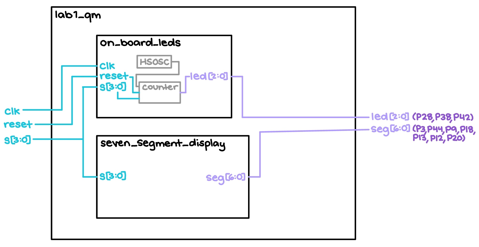
The block diagram in Figure 1 depicts the general architecture implied by the SystemVerilog code. The top-level module, titled “lab1_qm,” comprises two submodules, “on_board_leds” and “seven_segment_display” — the former for flashing the development board LEDs as detailed in the Introduction above, and the latter for recreating hexadecimal digits on the 7-segment display.
Schematic
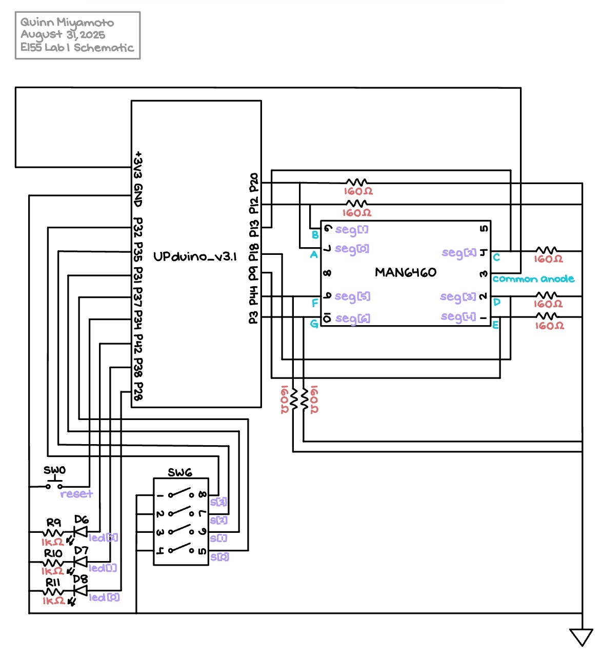
The Figure 2 schematic outlines how the physical components actually connect. More explicitly, the UPduino_v3.1 FPGA pins demonstrably feed and receive information from both the on-board elements — including a push-button, four slide-switches, three LEDs, and corresponding resistors of pre-determined 1 kΩ values — and the external MAN6460 7-segment display. Note that the values of the resistors connected to the 7-segment display were calculated by doing the following computations in Figure 3:
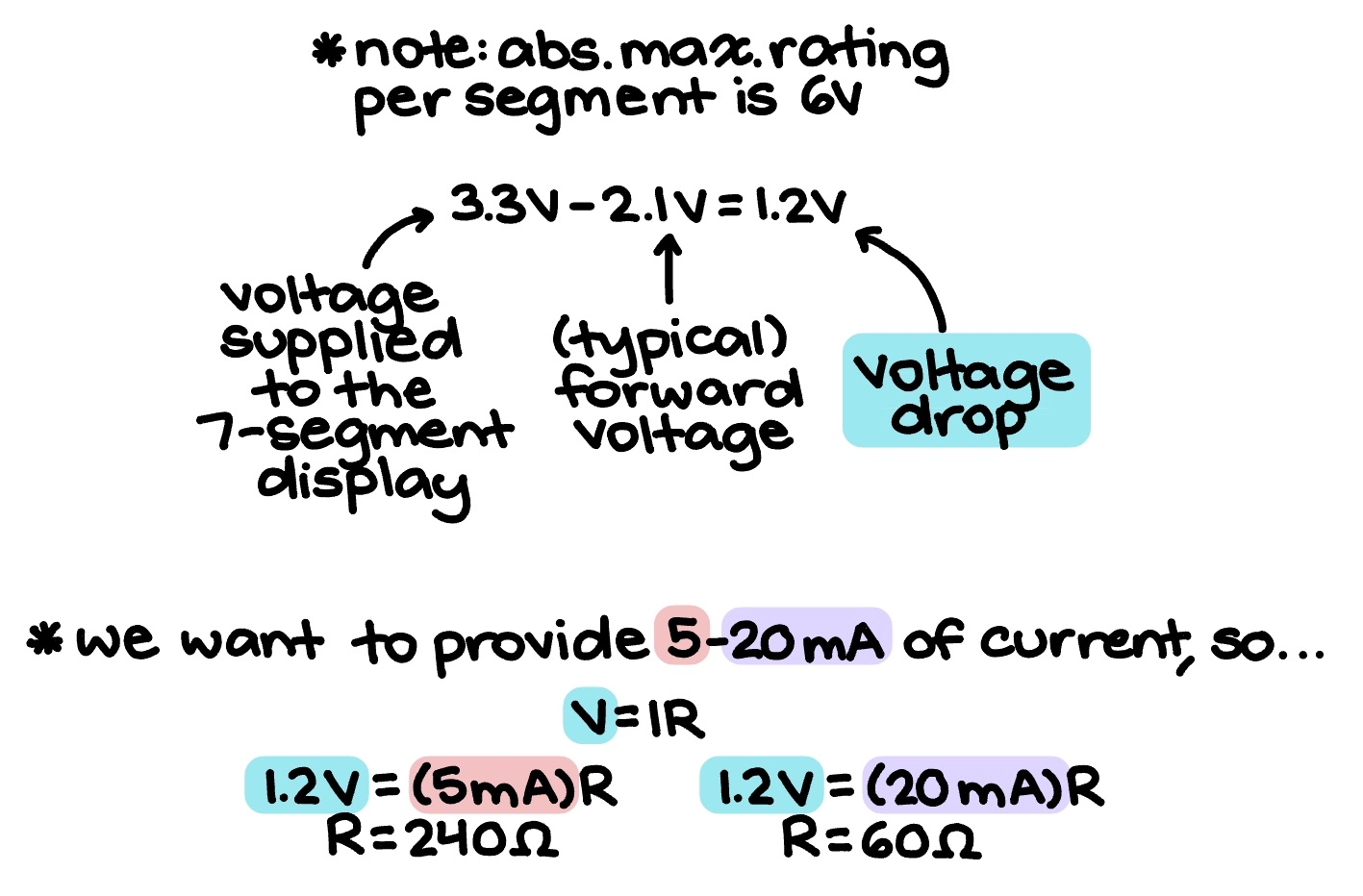
In order to attain current draw that fell within the recommended operating conditions of 5 - 20 mA, Ohm’s Law was applied to ultimately determine that any resistors ranging from 20 Ω to 240 Ω were acceptable to use. For the sake of equal brightness across all segments, seven 160 Ω-resistors were integrated into the Figure 2 schematic.
Results and Discussion
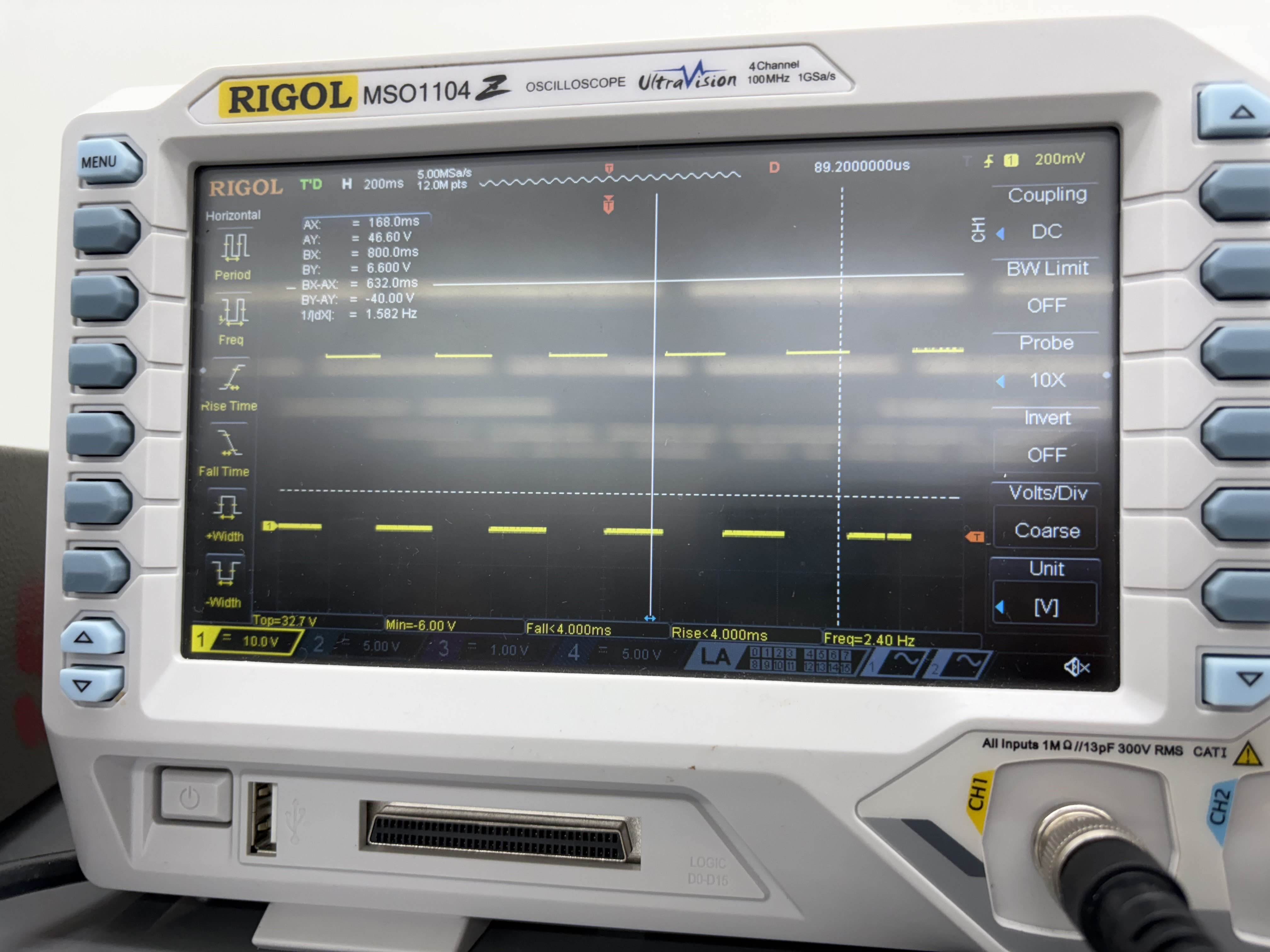
The results of Lab 1 can be viewed in Figure 4 below:
Evidently, all prescribed tasks were successfully accomplished, and the design performed quickly and reliably. Additionally, the oscilloscope trace from Figure 5 verified that one of the on-board LEDs did, in fact, flash at a constant rate of 2.4 Hz.
Testbench Simulation
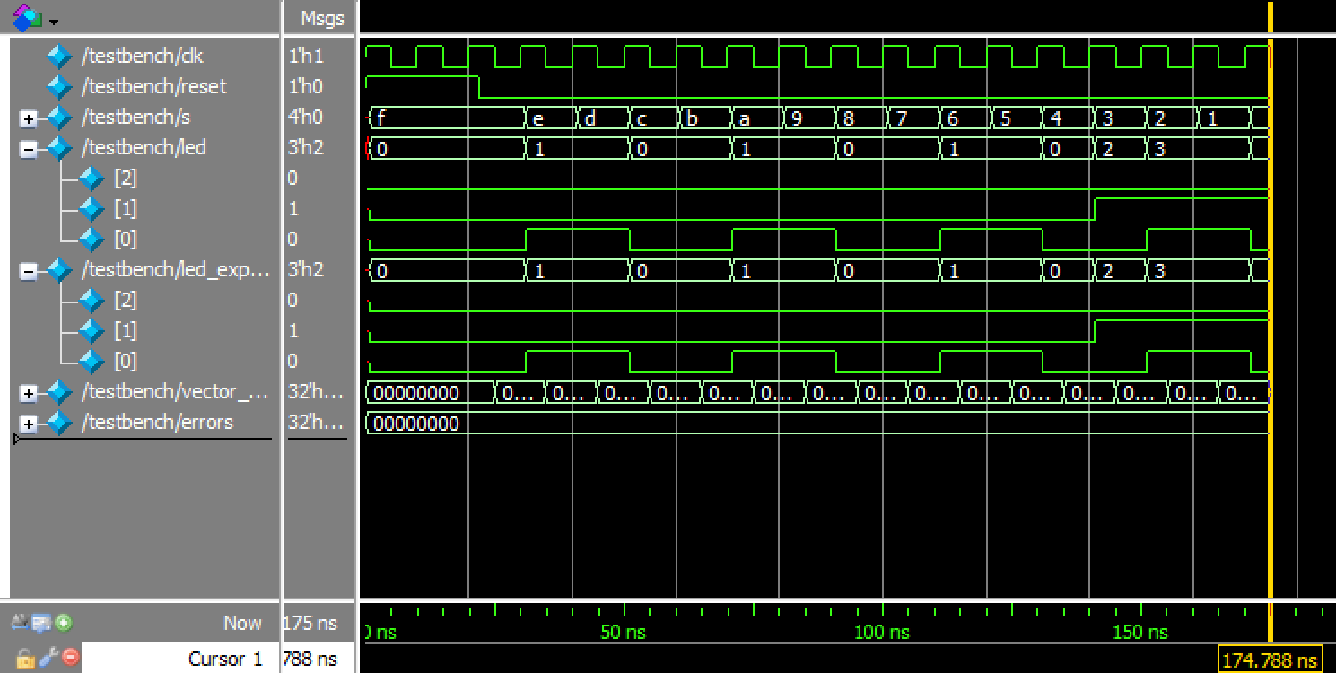
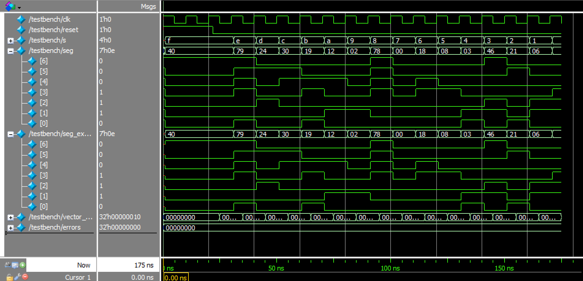
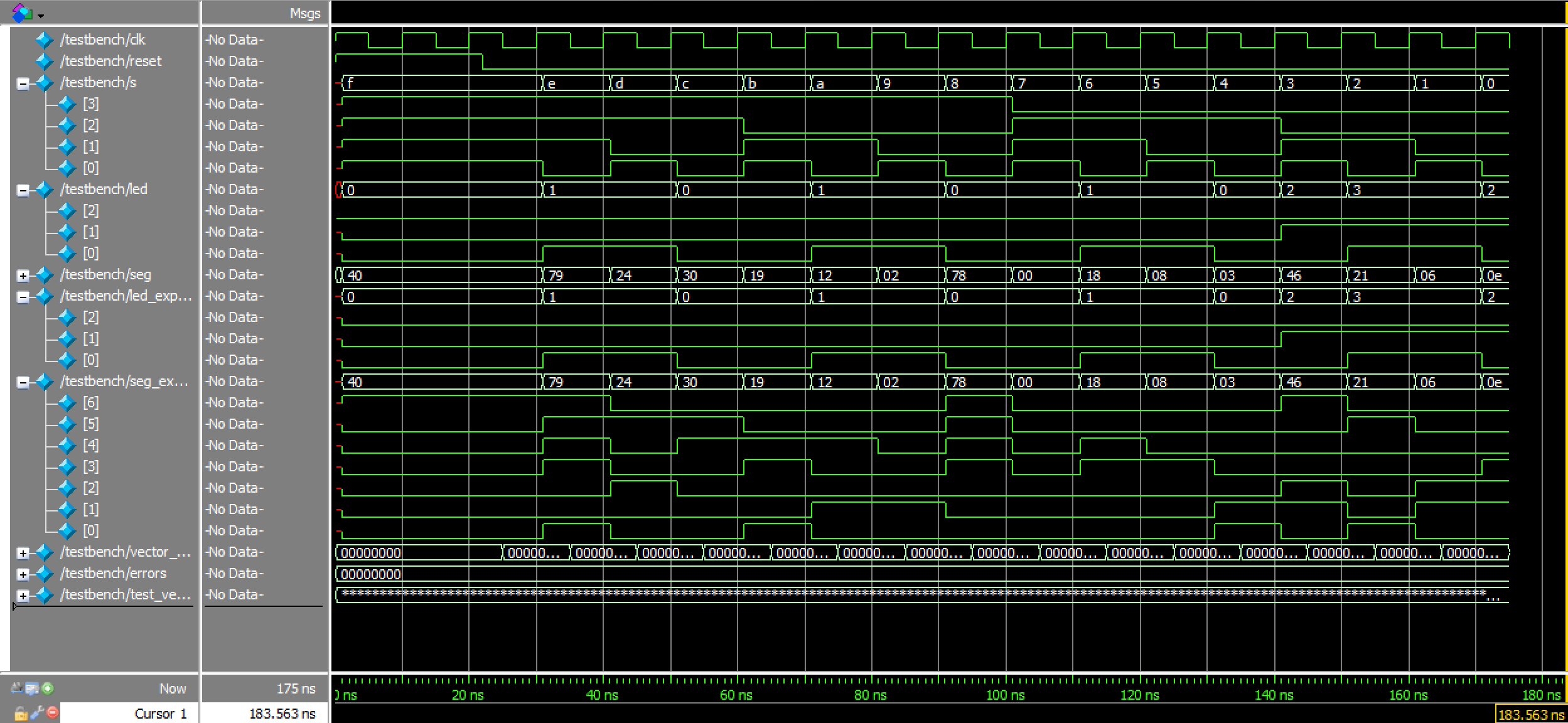
Moreover, the identical waveforms in Figures 6a, 6b, and 6c, as well as the terminal output of the cumulative, top module tests depicted in Figure 7, further prove that everything was working as intended.
Conclusion
In summary, the design flashed one on-board LED at a consistent 2.4 Hz, and configured four slide-switches with two other LEDs to create a XOR gate and AND gate, respectively. Furthermore, those same slide-switches successfully replicated every single hexadecimal digit on a 7-segment display, with each number sharing equal brightness. A total of approximately 25 hours was spent working on this lab.
AI Prototype
Using ChatGPT to generate some code in response to the prompt “Write SystemVerilog HDL to leverage the internal high speed oscillator in the Lattice UP5K FPGA and blink an LED at 2 Hz. Take full advantage of SystemVerilog syntax, for example, using logic instead of wire and reg,” the LLM ultimately produced inaccurate results that were unable to be synthesized; these can be viewed in the associated GitHub repository folder. While at first glance, the instructions in the chat transcript seemed rather straightforward and clear, when actually attempting to implement them in Lattice, there were many errors that popped up. After three tries at steering the LLM’s responses toward more accurate, desirable outcomes, all attempts at further guiding stopped.

The first error message received, as shown in Figure 8, concerned the missing iCE40UP primitive library file that was necessary for utilizing the SB_HFOSC module (in order to work with the development board’s high-frequency oscillator). This was addressed by taking ChatGPT’s “alternative workaround” recommendation to add an ifndef SYNTHESIS wrapper to the SB_HFOSC code to synthesize without adding extra files to the simulation. Unfortunately, while doing this did indeed get rid of the initial error, it led to the generation of another one.

Figure 9 depicts an error message pertaining to a “synthesis-time combinational loop error,” according to CHatGPT, which would supposedly be solved by re-checking the inclusion of the iCE40UP library and keeping ports tied correctly. However, this time, adhering to its directions did not have any effect on the synthesis.
The last error message to appear, as can be viewed in Figure 10 above, was the exact same as the one from Figure 9. At this point, ChatGPT presented the same solution for a third time, and was subsequently sidelined in favor of manually reviewing its code to fix things up.
In general, using an LLM to write the Lab 1 code was helpful to a certain extent; ChatGPT gave a rather good outline of what should be done to blink an LED at 2 Hz. However, when it came to the fine details that were crucial for making the code work, it tended to falter in supplying both adequate code and sufficient instructions for how to remedy any lapses in judgement. Therefore, the quality of the output was solidly middling.
Perhaps the most notable feature of the LLM’s code was its usage of the SB_HFOSC module, which was extremely similar to the HSOSC one actual utilized for the lab (as briefly talked about above). In the future, if LLM assistance is ever required by a project, more care will be taken to understand the constructs/syntax it employs so as to prompt it to give better, more effective answers.