Lab 2: Multiplexed 7-Segment Display
Introduction
In this lab, a time-multiplexer was implemented to switch between supplying power to two separate 7-segment displays, both of which were supposed to present a different hexadecimal digit (ranging from 0x0 to 0xF), depending on the positions of the four slide-switches assigned to them, respectively. Additionally, the multiplexing was to occur so quickly that the change would be imperceptible to the human eye; in this case, the frequency chosen was 100 Hz, and was generated using the 48 MHz internal high-speed oscillator and a corresponding clock divider. To achieve this more complicated arrangement, two transistors were integrated into the circuit to drive the large current required to fully power the 7-segment displays with the FPGA pins that would not necessarily be able to do so otherwise. The sum of both hexadecimal digits at any given point in time was then communicated in binary across five green, externally-wired LEDs.
Design and Testing Methodology
Overall, there were two inputs — including a reset (reset) and the eight slide-switches (switch[7:0]) — to the design and three outputs — that controlled the five LEDs (led[4:0]), each segment of the 7-segment displays (segment[6:0]), and the two transistors (transistor[1:0]), respectively.
As explained in Lab 1, the on-board high-speed oscillator, by default, produces a clock signal of 48 MHz. By implementing a clock divider with a counter that would toggle one transistor on and the other off every time it reached 240,000 — because 48 MHz divided by the desired 100 Hz (as previously mentioned above) results in 480,000, and the toggling should take place twice a cycle (therefore dividing 480,000 by two to get 1240,000) — the time-multiplexing was able to occur at the correct frequency. Note that the value of 100 Hz was chosen arbitrarily at first, before being deemed acceptable after observing the physical circuit in action and being unable to identify any noticeable delay and bleeding.
Regarding the 7-segment display design, as with Lab 1, each hexadecimal digit was intentionally designed to have a distinct appearance. Because there were not enough FPGA pins to drive each segment individually across the two displays, there was simply one pin assigned to each unique pair of segments (for example, one pin would drive the bottom-left segments of both displays). Thanks to the lab’s multiplexing design, this was able to be done with no confusion as to which pins should be activated when.
Various tests were conducted on the final product, including both physical interaction with the resultant circuits and simulation testbenches, as elaborated on in a later Results and Discussion section. Note that there was an individual testbench created for each SystemVerilog module.
Technical Documentation
The source code for this project can be found in the associated GitHub repository folder.
Block Diagram
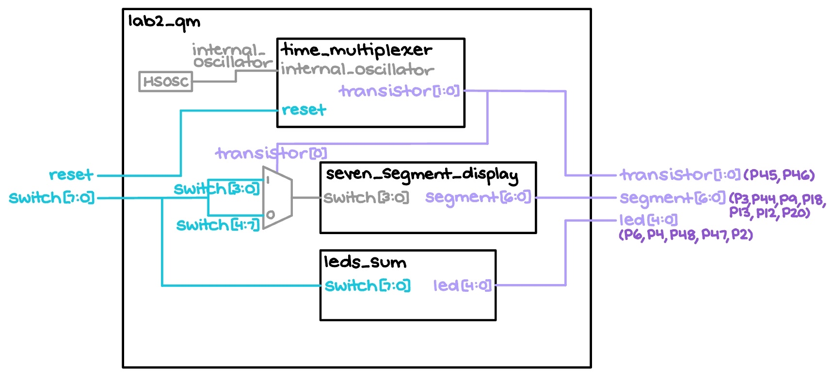
The block diagram in Figure 1 depicts the general architecture implied by the SystemVerilog code. The top-level module, titled “lab2_qm,” comprises a high-speed oscillator module that generates an internal_oscillator signal that supplies a clock for the following “time_multiplexer” module, which alternates the activation status of the two transistors. That module is then followed by a mux, which chooses which set of four switch inputs to send to the “seven_segment_display” module and recreate hexadecimal digits, depending on the transistor that is on at the time; “seven_segment_display” can only handle four switch inputs at once, as it is an exact copy of the Lab 1 one’s design. Finally, the “leds_sum” module adds the two hexadecimal digits together and conveys the binary sum accordingly.
Schematic
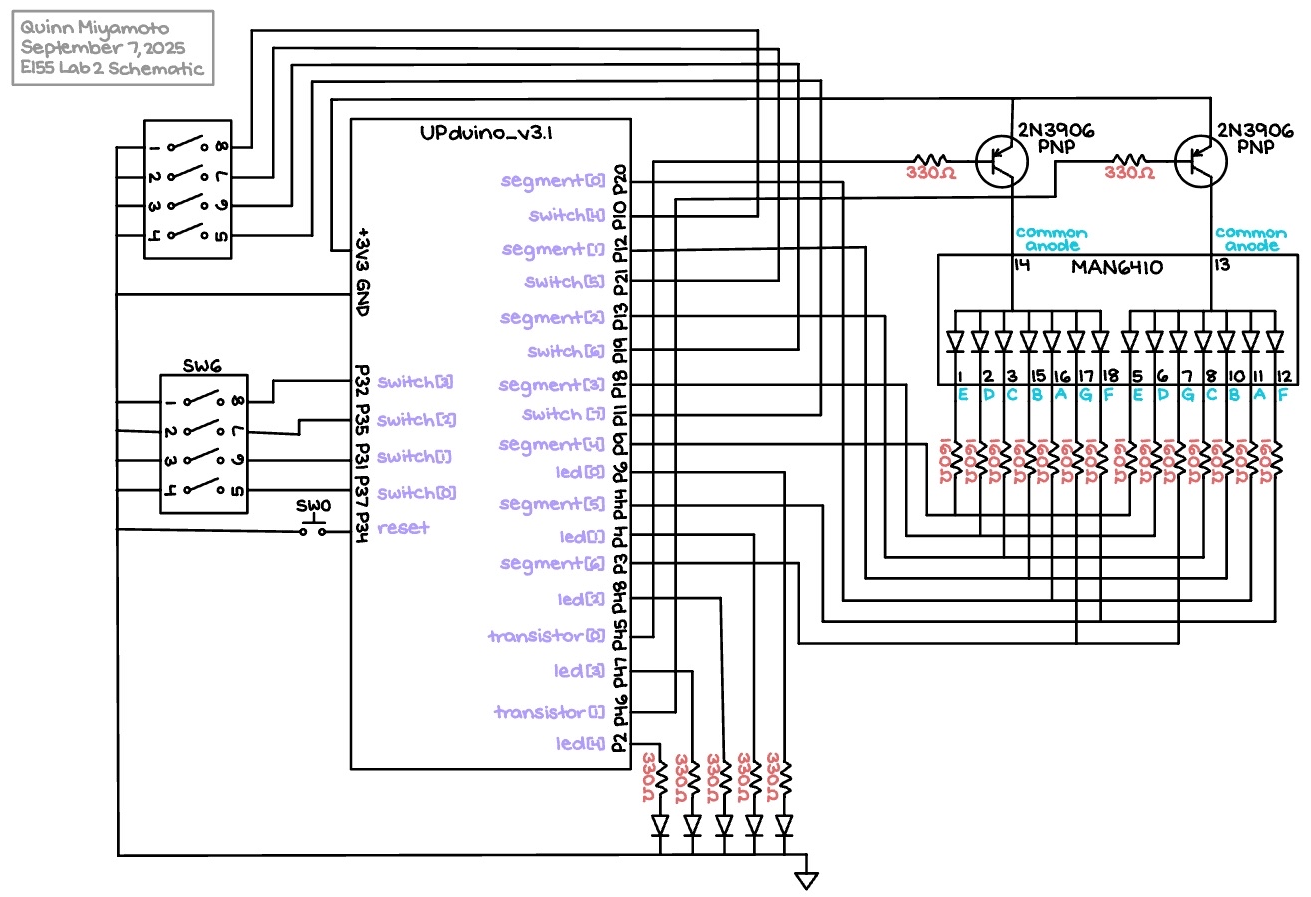
The Figure 2 schematic outlines how the physical components actually connect. More explicitly, the UPduino_v3.1 FPGA pins demonstrably feed and receive information from both the on-board elements — including a push-button and four slide-switches — and the external MAN6410 7-segment displays, two 2N3906 PNP transistors, four additional slide-switches, five LEDs, and resistors of variable values.
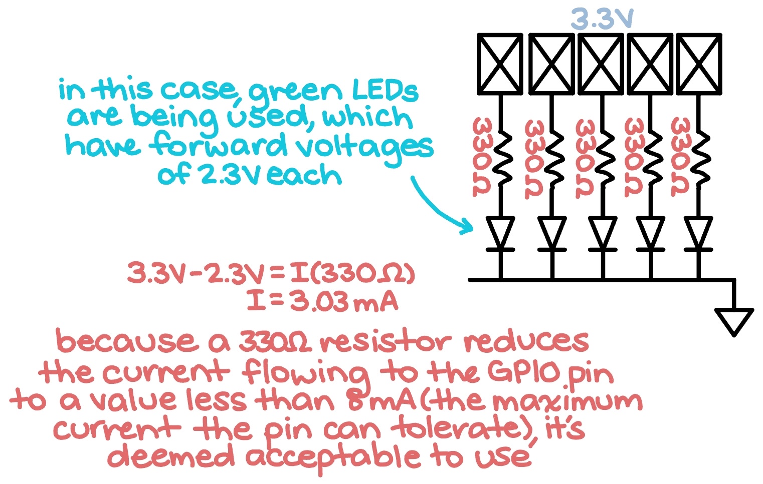
Regarding the latter, firstly, note that the values of the resistors connected to the two transistors and the two 7-segment displays, respectively, were picked after doing the computations depicted in Figure 3 below:
As specified in section 4.17 of the ice40 datasheet for the FPGA, the current flowing into each GPIO pin should ideally be 8 mA at most. Thus, to justify the the particular resistors chosen, Ohm’s Law was applied to each part of the zoomed-in segment of the main circuit, clearly demonstrating that all current draw fell within recommended operating conditions. Ultimately, for the sake of equal brightness across all segments, seven 160 Ω-resistors were integrated into the 7-segment display circuit, while both transistor bases received current-limiting resistors of 330 Ω. (Sources for the cited transistor information above comprise SparkFun Electronics and Glenn Lockwood. Additionally, the 7-segment display datasheet was used to find the forward voltage necessary to complete the correct calculations.)
Moreover, the use of one 330 Ω-resistor per green LED can be rationalized via the following Figure 4:
Results and Discussion
The results of Lab 2 can be viewed in Figure 5 below:
Evidently, all requirements were met. While the camera could detect some flickering that the naked human eye cannot perceive, it can still be conclusively said that the design was extremely effective.
Testbench Simulation
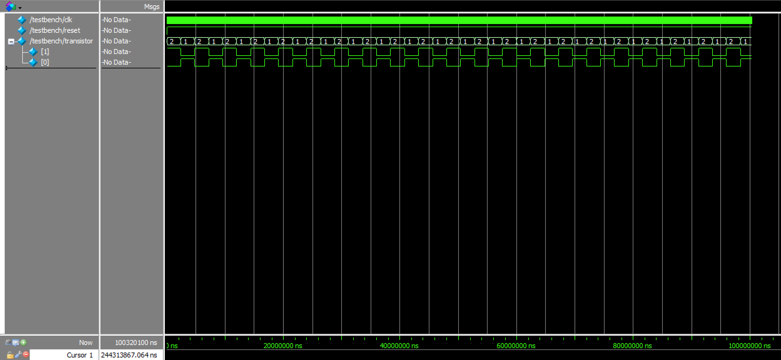
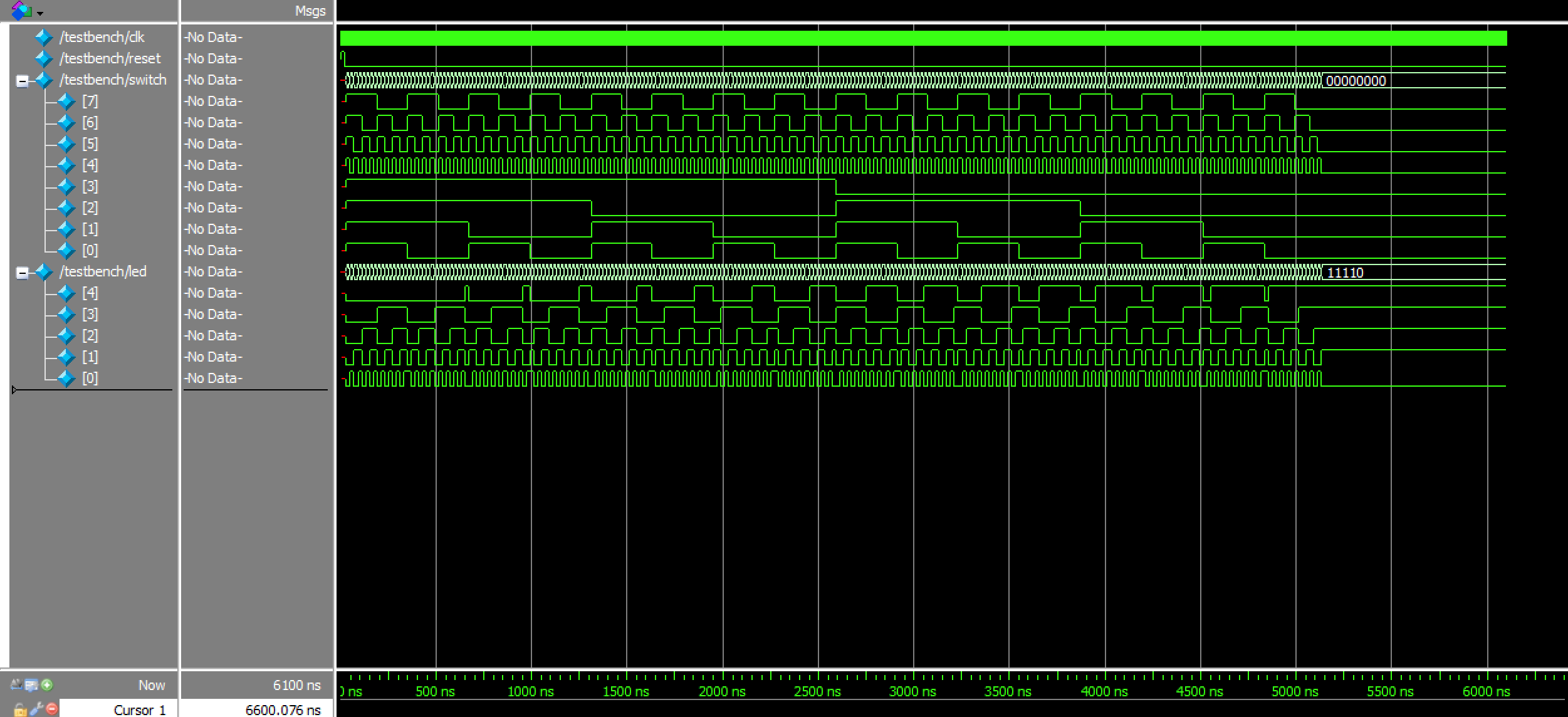
The waveforms in Figures 6a, 6b, and 6c further verify that the design was working exactly as intended; the time-multiplexing module toggles both transistors on and off at opposite times, the sums displayed across the LEDs always match the expected outcomes, and the top module hooks everything up to change with both the switch inputs and transistor activations as necessary.
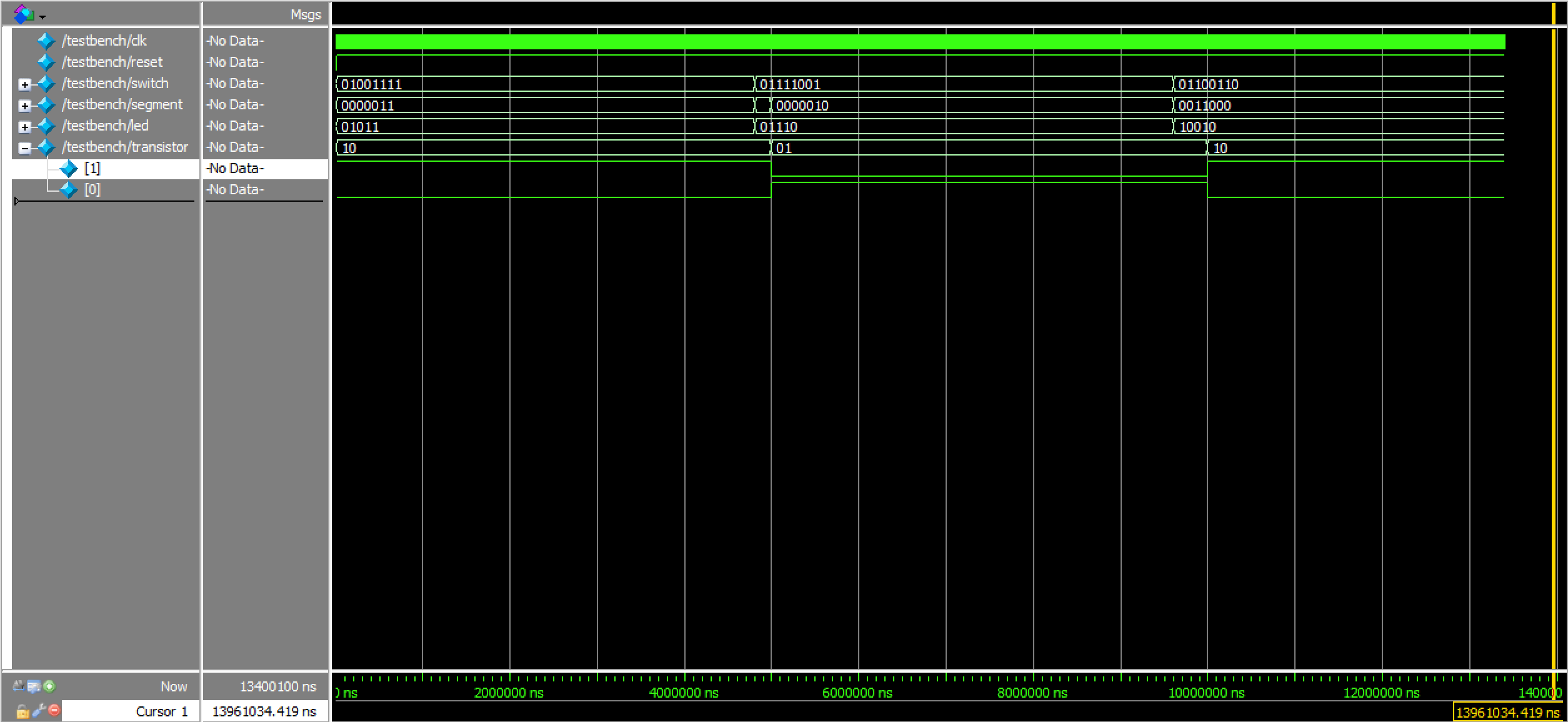
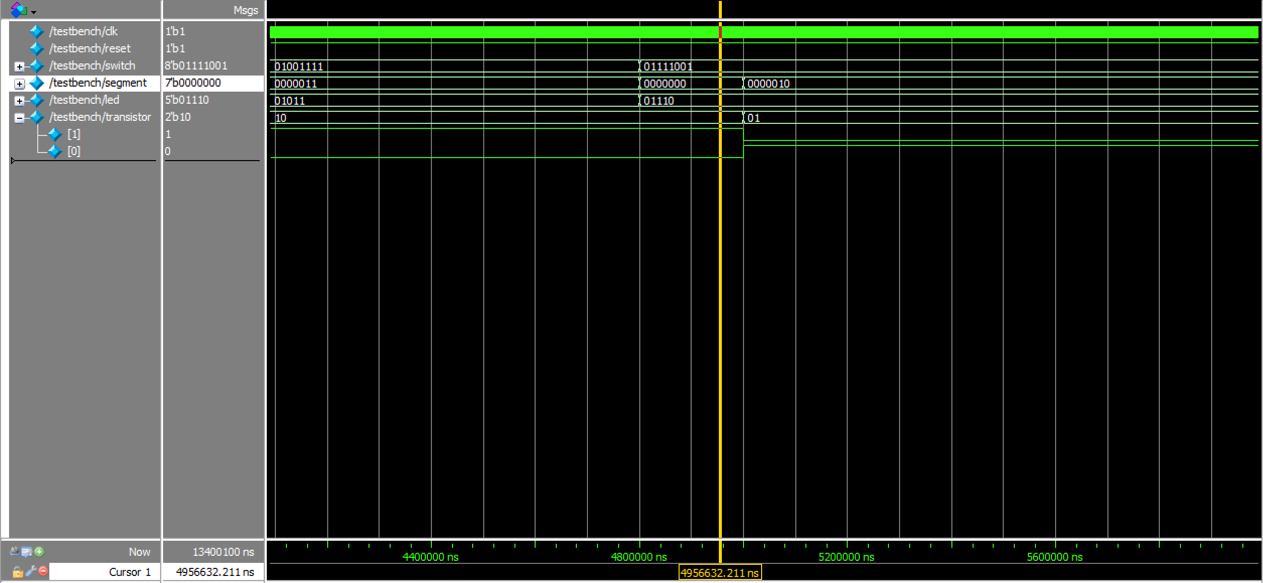
To go more in depth about the top module waveforms, first note that the switch inputs are not changing at the exact same time as the transistors. This was intended to model more real-world behavior, in which someone would never realistically be moving the switches directly in sync with the rising edge of the internal clock. Furthermore, there is a small, indiscernible region around the 5,000,000 ns mark. This can be viewed more clearly in Figure 7 as follows:
As can be observed in the Figure 1 block diagram, there was also a 7-segment display module used that — by proper verification standards — should have been simulated. It can be seen in Figure 8 below. Note that it is the exact same as the 7-segment display module used in Lab 1.
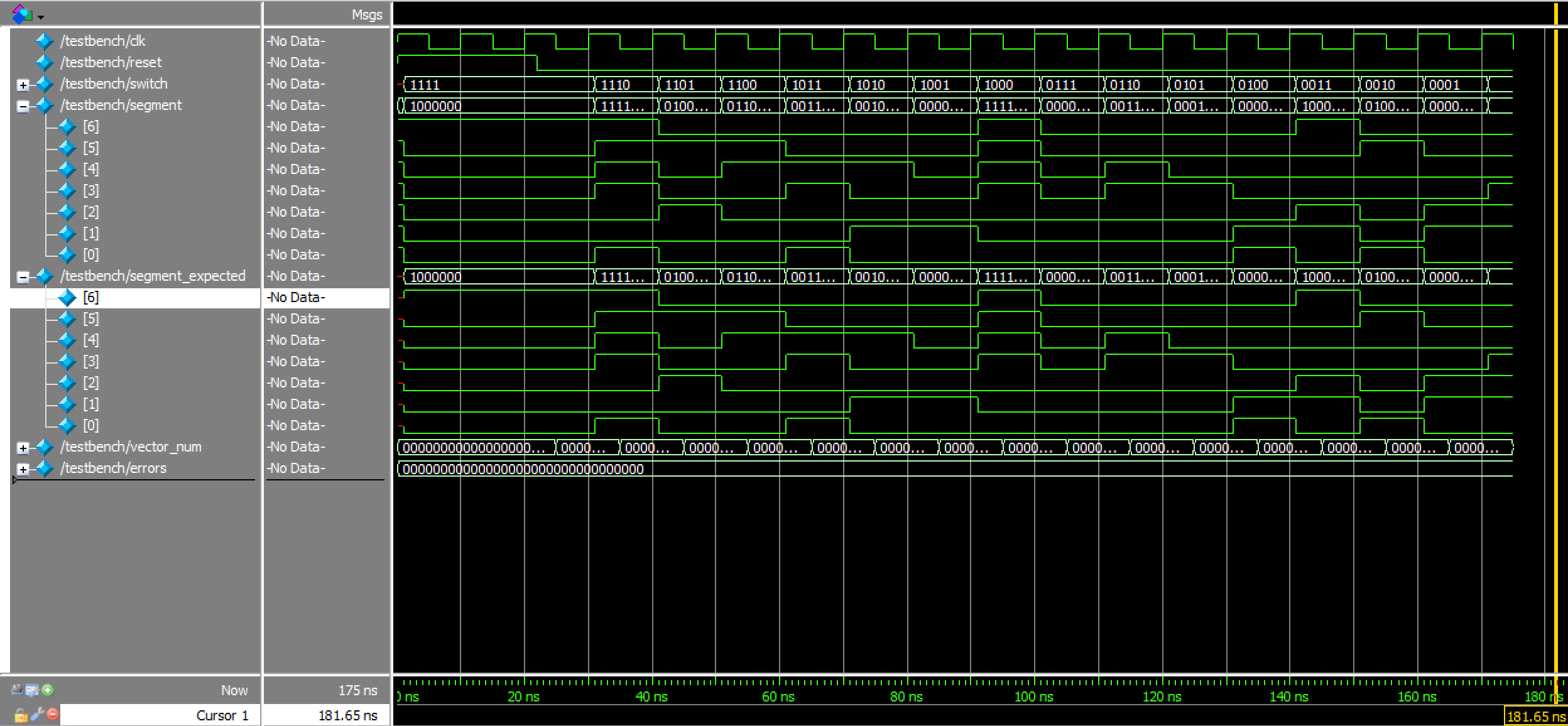
All testbenches and simulations passed without the presence of any error messages.
Conclusion
In summary, the design toggled two 7-segment displays on and off at a constant 100 Hz with the help of transistors, such that they would always appear to depict two hexadecimal digits at once. These 7-segment displays were properly interfaced with four slide-switches each (for a total of eight slide-switches incorporated into the circuit overall), with the respective outputs dependent on the positions of said switches. Furthermore, the sum of both digits was consistently depicted in binary across five LEDs. A total of approximately 12 hours was spent working on this lab.
AI Prototype
Using ChatGPT to generate some code in response to the prompt “Write SystemVerilog HDL to time multiplex a single seven segment decoder (that decodes from four bits to a common anode seven segment display) to decode two sets of input bits and drive two sets of seven output bits,” the LLM produced results that surprisingly synthesized; these can be viewed in the associated GitHub repository folder. Additionally, the full response can be seen in the public chat transcript.
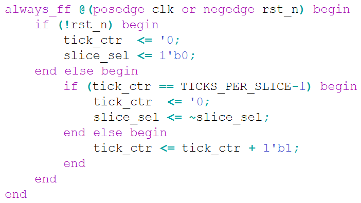
While the AI utilized a lot of unfamiliar code in its module, the general logic seemed to make sense. It used the same sort of counter-driven flip-flopped-toggle logic (see Figure 9) that was employed in the actual Lab 2 design to time-multiplex the two 7-segment displays, with a single set of case statements acting as a decoder, as requested.
Furthermore, in response to the second prompt, “Write SystemVerilog HDL to time multiplex a single seven segment decoder (that decodes from four bits to a common anode seven segment display) to decode two sets of input bits and drive two sets of seven output bits. Use the seven segment decoder and oscillator provided in the attached files,” ChatGPT once again generated seemingly satisfactory results. The full response to this prompt can be seen in a second, entirely separate chat transcript.
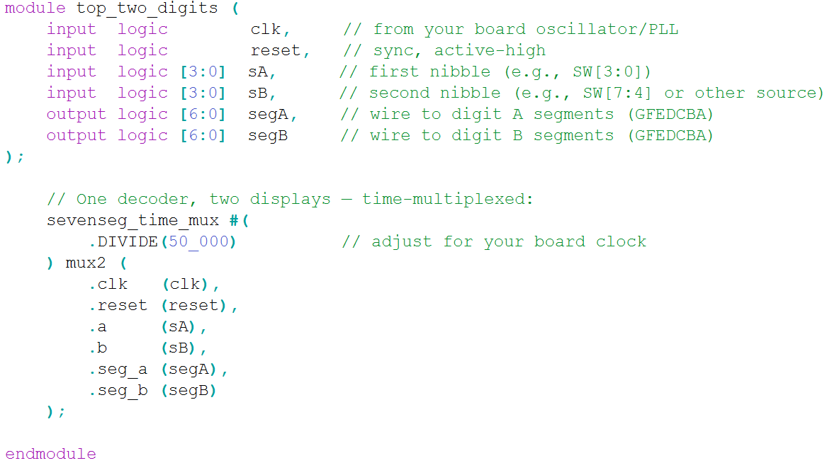
As with its first response, this new code also contained new Verilog idioms, but still synthesized on the first try. Upon closer inspection, it once again appeared that the AI’s overall plan for tackling the prompt was correct. This time, it even provided a complementary top module for the code, albeit a somewhat unnecessary one, as shown in Figure 10 below:
Overall, the quality of the output was acceptable, as it seemed to be mostly accurate after a cursory glance. In general, using an LLM to write the Lab 2 was genuinely helpful; it gave both a solid approach to solving the problem and code that did not generate any immediate errors in response to attempted implementation. However, in future projects for which LLM assistance is required, asking for additional, more explanatory comments as to what the employed Verilog idioms mean might make its answers even more useful.