Lab 3: Keypad Scanner
Introduction
This lab built upon the time-multiplexed 7-segment display setup from the previous Lab 2, introducing the additional complication of integrating a 4x4 matrix keypad so that its two most recent key presses would subsequently register on said 7-segment displays. More specifically, the value of the latest key press needed to show on the rightmost display and shift left every time a new input was received, with sufficient compensation for switch bouncing. Note that after an initial key press, the design was required to ignore all following presses until the first had been released. In order to accomplish this, there needed to be robust digital design that could account for the asynchronous nature of all user interactions with the circuit, such that they would not disrupt the outputs and general flow of the remaining synchronized components. Moreover, the design could not comprise any latches or tristate buffers.
Design and Testing Methodology
Overall, there were two inputs — including a reset (reset) and four keypad columns (keypad_column[3:0]) — and three outputs — a row activator (keypad_row[3:0]), transistor toggler (transistor[1:0]), and 7-segment display setter (segment[6:0]) — to the design.
Using the default 48 MHz clock produced by the internal oscillator and dividing it to get a slower 24 MHz one, this new signal was fed into an FSM and nested synchronizer. The synchronizer delayed the usage of the keypad_column signal by two cycles in order to mitigate metastability (by providing settling time for any in-between values to stabilize) and meet the aforementioned requirement of asynchronous input-handling.
Additionally, as with Lab 2, the 24 MHz clock signal was used to alternate the activation of both transistors at a rate of 100 Hz, which then drove the 7-segment display outputs. Each hexadecimal digit of the 7-segment display was intentionally designed to have a unique appearance. This was reflected in the Verilog code via unique case statements with one toggle-able pin assigned to each segment.
Furthermore, although the exact workings of the FSM are explained in greater detail down below, know that its most notable features were: 1) the use of both a flip-flop and case statement to store and toggle the FSM’s inputs, outputs, and intermediate signals all at once, and 2) its switch-debouncing strategy. Regarding the former, it was found that it was easiest to just combine the output and state transition signals into one giant module, as it made both conceptually tracking everything and the following, inevitable debugging easier on the programmer. Additionally, when considering the latter, there were a variety of ways that the design could have manifested; however, the final product saw the emergence of a waiting stage that only allowed the most recently and second most recently pressed key locations to update after 0.1 s had passed. This specific time period was chosen because it was deemed to be long enough that the switch bouncing would settle before it was over, but short enough that no additional button presses could occur throughout and be missed.
While there was an initial attempt made to implement a more rigorous method of debouncing involving counting each time a key went high for every single button at the same time, and eventually taking the key with the largest corresponding number as the official debounced result, there were a few concerns that led to that idea being discarded. Namely, the multiple timing violation errors that kept popping up, as well as the fact that this would be expensive and inefficient to implement in actual hardware, anyway.
Thus, the “sit-and-wait” strategy of debouncing manifested and eventually stuck. Its primary tradeoff is that it has a small delay when registering two or more keys that have been pressed in extremely rapid succession. However, because that is an edge case — that the design would still work for, just not as beautifully — and with the current method, there is relatively little hardware implied, a design decision was made to just keep it. If one really wanted to, they could even shorten the wait period to mitigate this “problem.”
Another miniscule tradeoff is that there is a tiny delay in the shifting of most recent and second most recent digits (something that is not considered as “clean” as other designs), as a byproduct of assigning the second most recent digit’s value before the most recent digit’s one in the aforementioned FSM. But, again, because this does not functionally compromise the design in any way, shape, or form, a design decision was ruled in favor of keeping everything the same.
Various tests were conducted on the final product, including both physical interaction with the resultant circuits and simulation testbenches, as elaborated on in a later Results and Discussion section. Note that there was an individual testbench created for each SystemVerilog module.
Technical Documentation
The source code for this project can be found in the associated GitHub repository folder.
Block Diagram
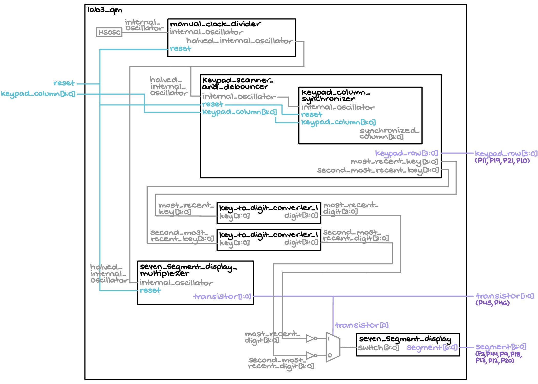
The block diagram in Figure 1 depicts the general architecture implied by the SystemVerilog code. The top-level module, titled “lab3_qm,” comprises a high-speed oscillator module that generates a 48 MHz signal, which is immediately halved in the ensuing “manual_clock_divider” block; this ultimately results in a 24 MHz halved_internal_oscillator clock that is fed to the rest of the time-dependent components. One such component is the “keypad_scanner_and_debouncer” module, which contains an FSM that first stabilizes the column inputs with a “keypad_column_synchronizer,” before determining and subsequently storing the locations of the two most recently pressed keys — all the while simultaneously accounting for debouncing (see below for more details). This then allows “key_to_digit_converter_1” to turn these saved locations into their corresponding hexadecimal values so that they may be interpreted by the “seven_segment_display” and turned into actual, illuminated outputs. Finally, the “seven_segment_display_multiplexer” module alternates the activation status of the two transistors that actually drive the 7-segment displays, and is immediately followed by a mux that decides which digit is showing at any given point in time.
Finite State Machine Design
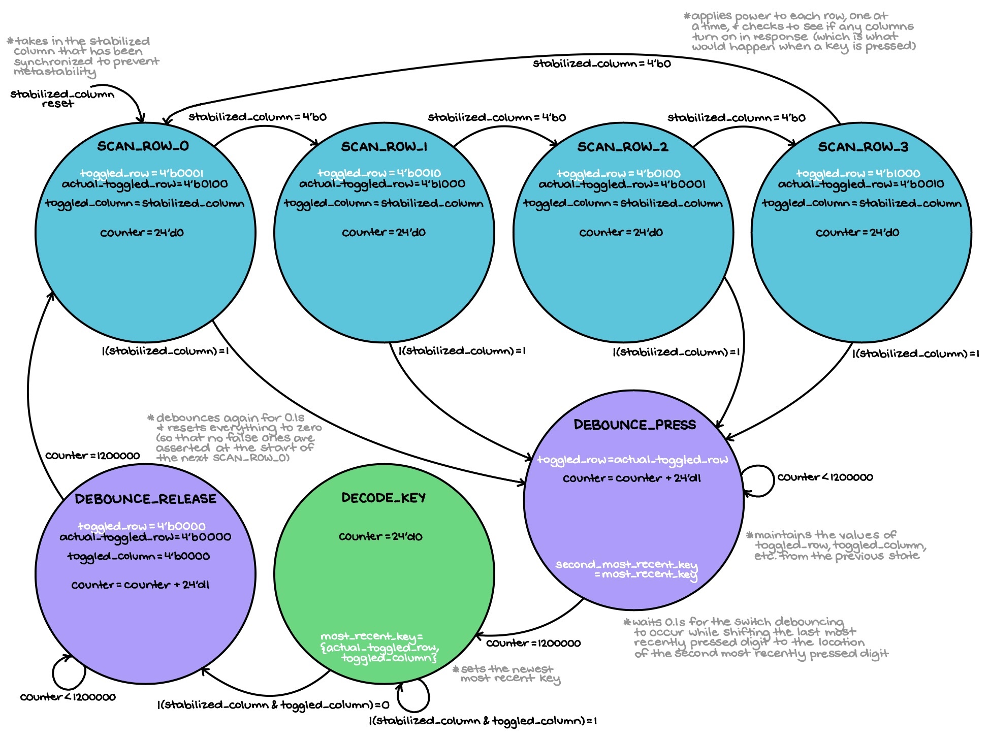
The Figure 2 FSM illustrates the seven main stages of key detection, switch debouncing, and digit shifting based on recency. Note that the actual Verilog implementation of this FSM is not quite standard, but effective in reaching the end goal nonetheless. After parsing both the code and diagram for the specific signals being toggled, the following Figures 3a and 3b were created for ease of understanding and general transition-tracking.
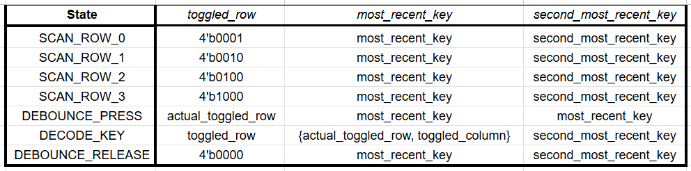
In short, the FSM supplies powers to each row of the keypad, one at a time, until it detects that a column has toggled high in response and moves on; this indicates a key press. Because the column signals have gone through a synchronizer that imposes upon them a two-cycle delay, however, there is a variable actual_toggled_row that accounts for the fact that the rows should actually be offset, as well. Thus, actual_toggled_row stores the row that would have been high two cycles ago when it synced up with the detected column.
Following the scanning stages, the FSM contains a switch-debouncing state that forces the entire system to wait for 0.1 s, therefore allowing any sort of short, echoing “bounces” to settle before proceeding to take the registered input as fact. In this state, the value of what was previously considered the most recent key press is shifted to the left to take the second most recent key press’ place.
Next, the FSM assembles the segmented row and column information that it has successfully accumulated and forms a more comprehensive key location. It then passes this off as the most recent digit, and waits until there are no more registered presses (between the saved toggled_column value that froze the moment a key press was asserted and any other buttons that may have been pushed in the meantime) to move on to the final stage.
Lastly, the FSM performs a second round of 0.1 s debouncing while resetting both the stored/asserted row and column values to zero, so as not to trigger any false button presses with residual high values when moving back to that very first scanning state.
Schematic

The Figure 4 schematic outlines how the physical components actually connect. More explicitly, the UPduino_v3.1 FPGA pins demonstrably feed and receive information from the on-board push-button, external MAN6410 7-segment displays, two 2N3906 PNP transistors, 4x4 Adafruit matrix keypad, and resistors of variable values.
Regarding the latter, firstly, note that the values of the resistors connected to the two transistors and the two 7-segment displays, respectively, were picked after doing the computations depicted in Figure 5 below:
As specified in section 4.17 of the ice40 datasheet for the FPGA (and previously mentioned in the Lab 2 documentation), the current flowing into each GPIO pin should ideally be 8 mA at most. Thus, to justify the the particular resistors chosen, Ohm’s Law was applied to each part of the zoomed-in segment of the main circuit, clearly demonstrating that all current draw fell within recommended operating conditions. Ultimately, for the sake of equal brightness across all segments, seven 160 Ω-resistors were integrated into the 7-segment display circuit, while both transistor bases received current-limiting resistors of 330 Ω. (Sources for the cited transistor information above comprise SparkFun Electronics and Glenn Lockwood. Additionally, the 7-segment display datasheet was used to find the forward voltage necessary to complete the correct calculations.)
Furthermore, the four pull-down resistors connected to the keypad columns — the top-level Verilog module’s inputs — have values of 1 kΩ, as the circuit in question is a speed-sensitive one.
Results and Discussion
The results of Lab 3 can be viewed in Figure 6 below:
Evidently, the design met all of the desired specs. While there were some miniscule compromises with regard to key-sensing/toggling speed that had to be made for the sake of more wholistic operation, nothing is objectively wrong with the chosen means of implementation.
Testbench Simulation
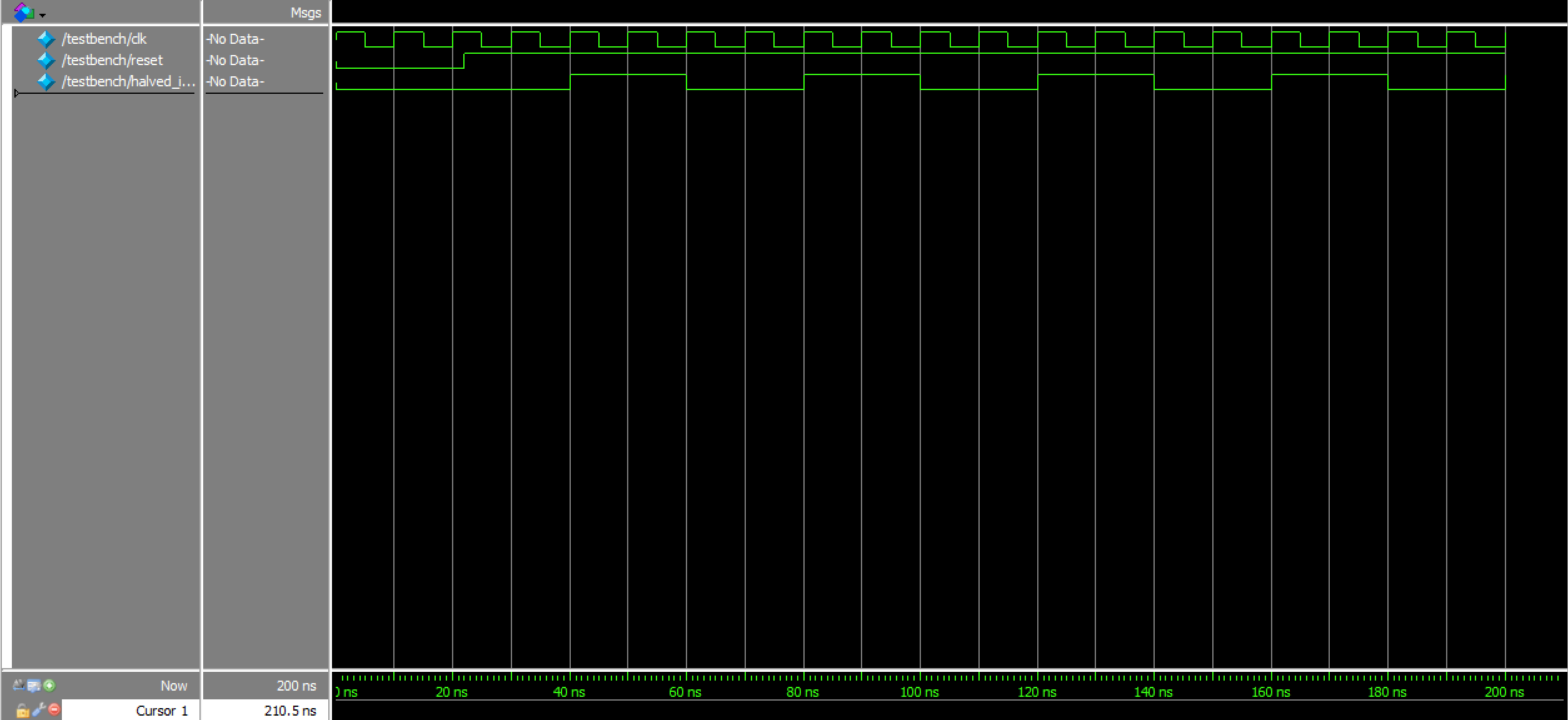
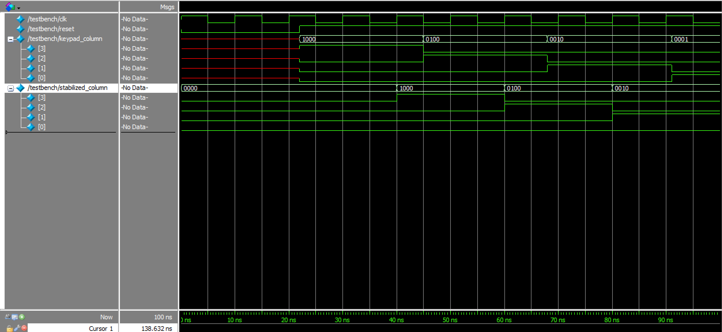
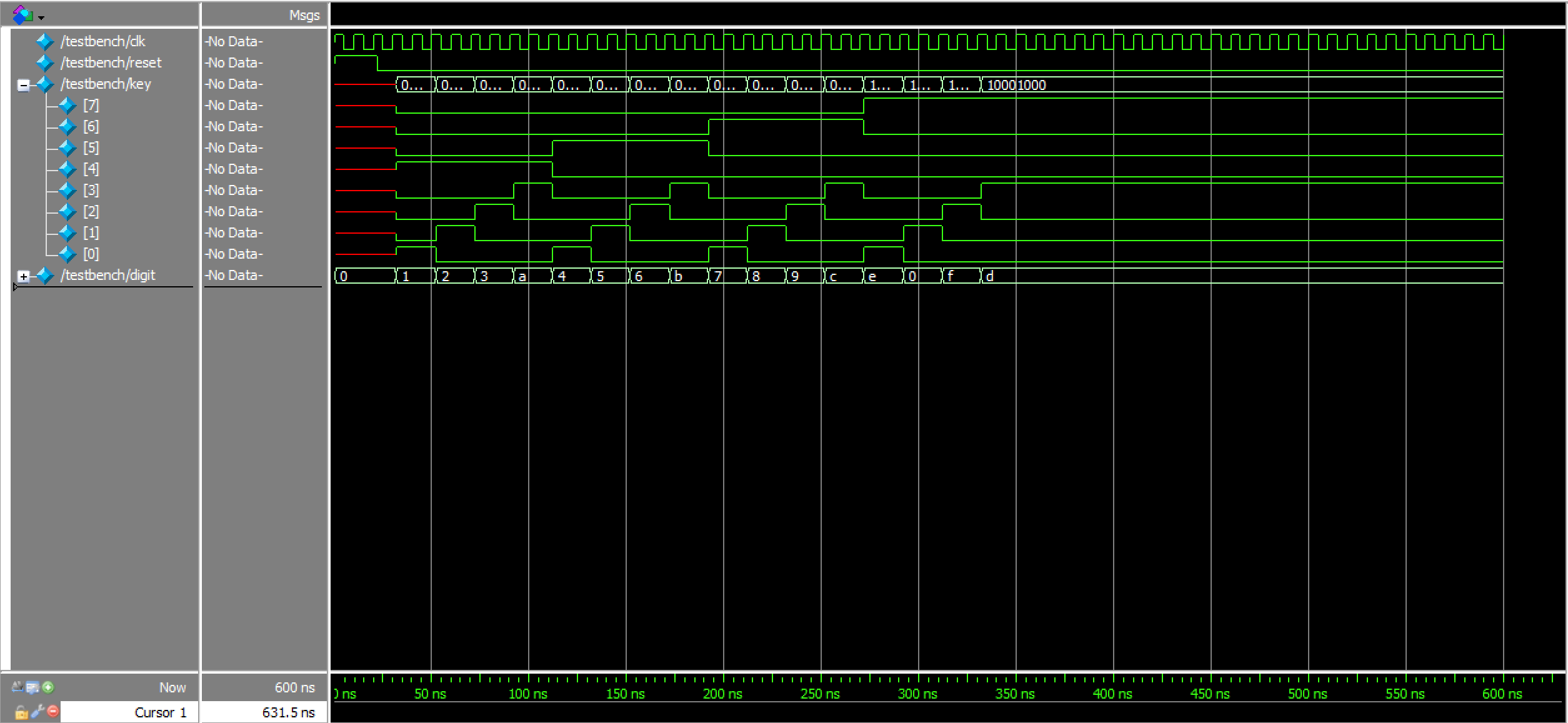
The submodule waveforms in Figures 7a, 7b, and 7c further verify that the design was working exactly as intended: the clock-divider waveforms proved that the halved_internal_oscillator signal took twice as long as the module’s input to complete a full clock cycle, the synchronizer waveforms showed that the keypad_column inputs were, in fact, being offset by two cycles before being returned as outputs, and the key-to-digit converter waveforms demonstrated that every single activated row-column pairing produced the correct hexadecimal digit.
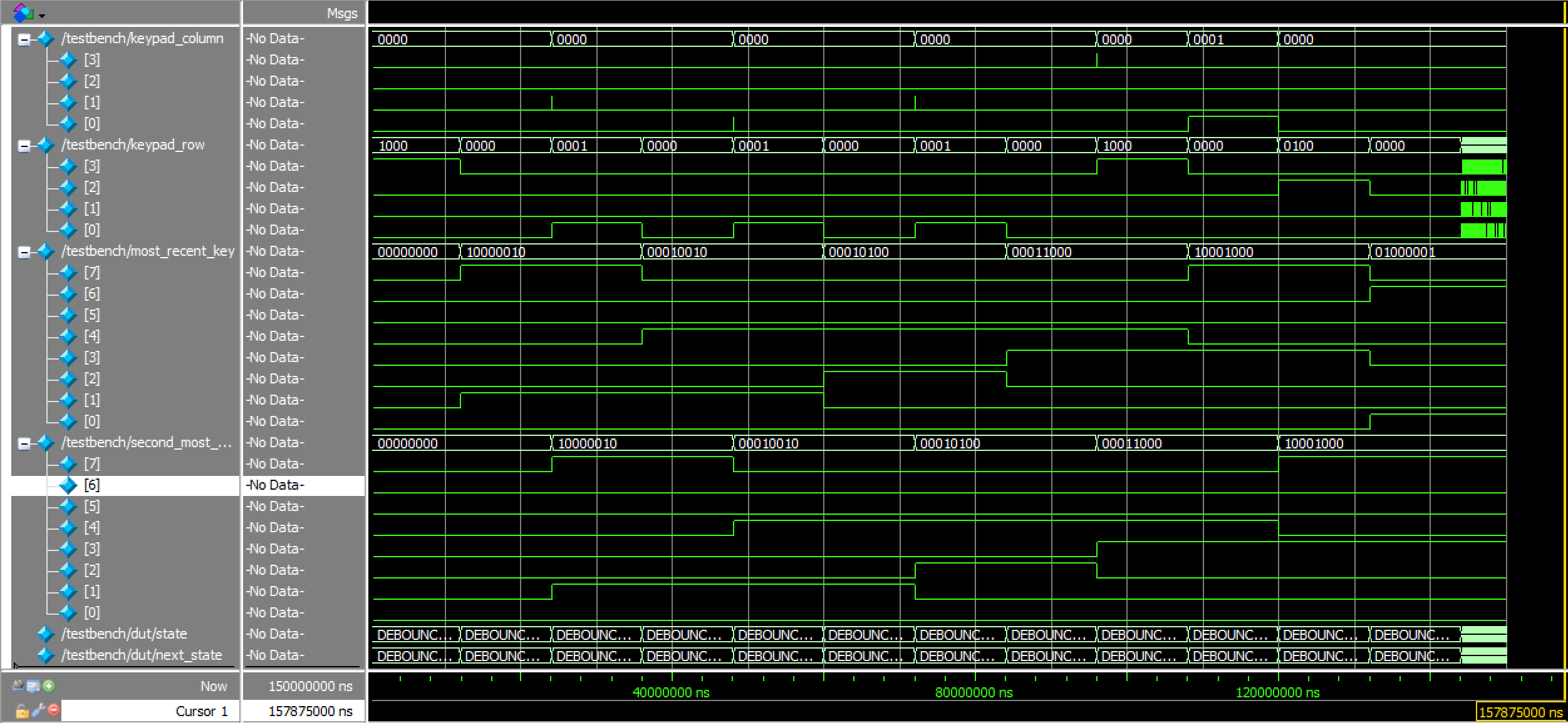
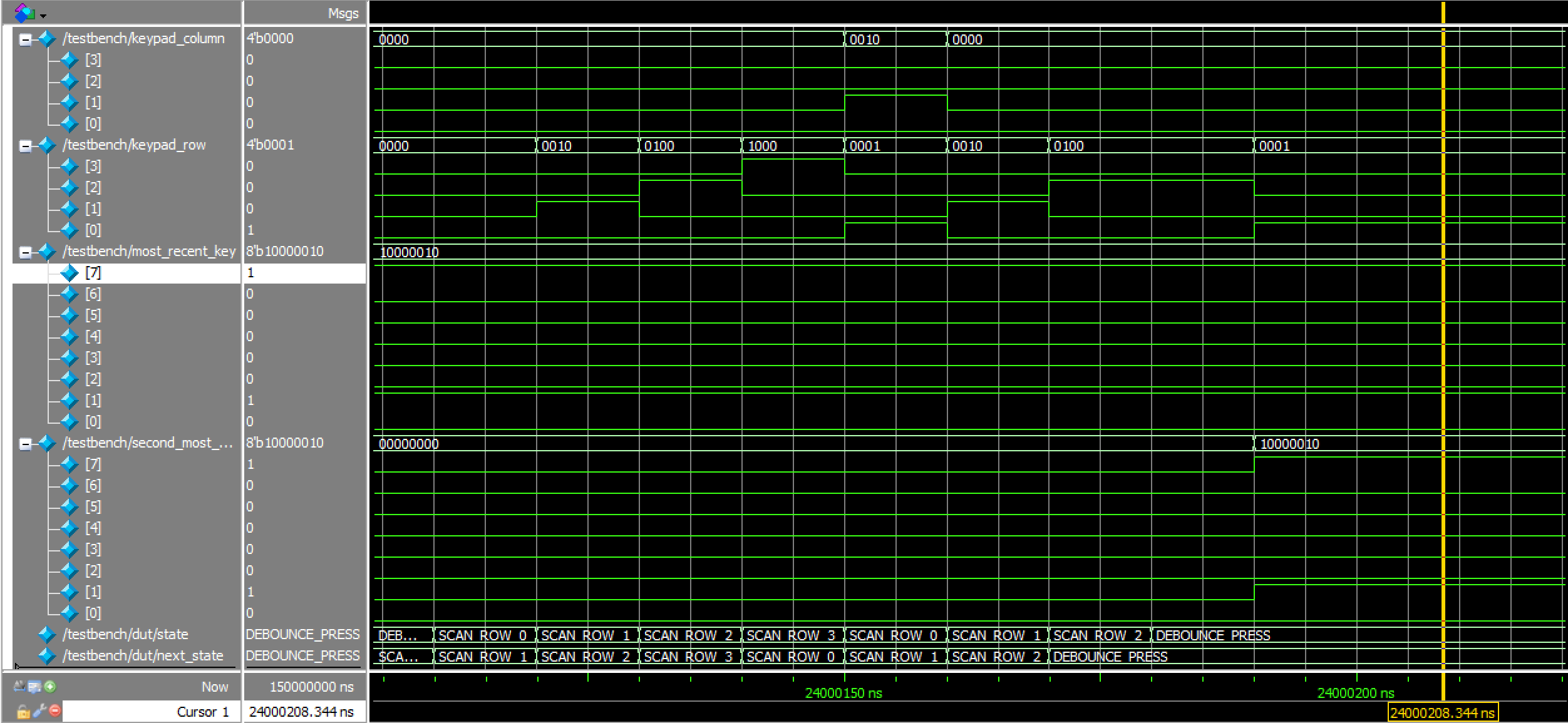
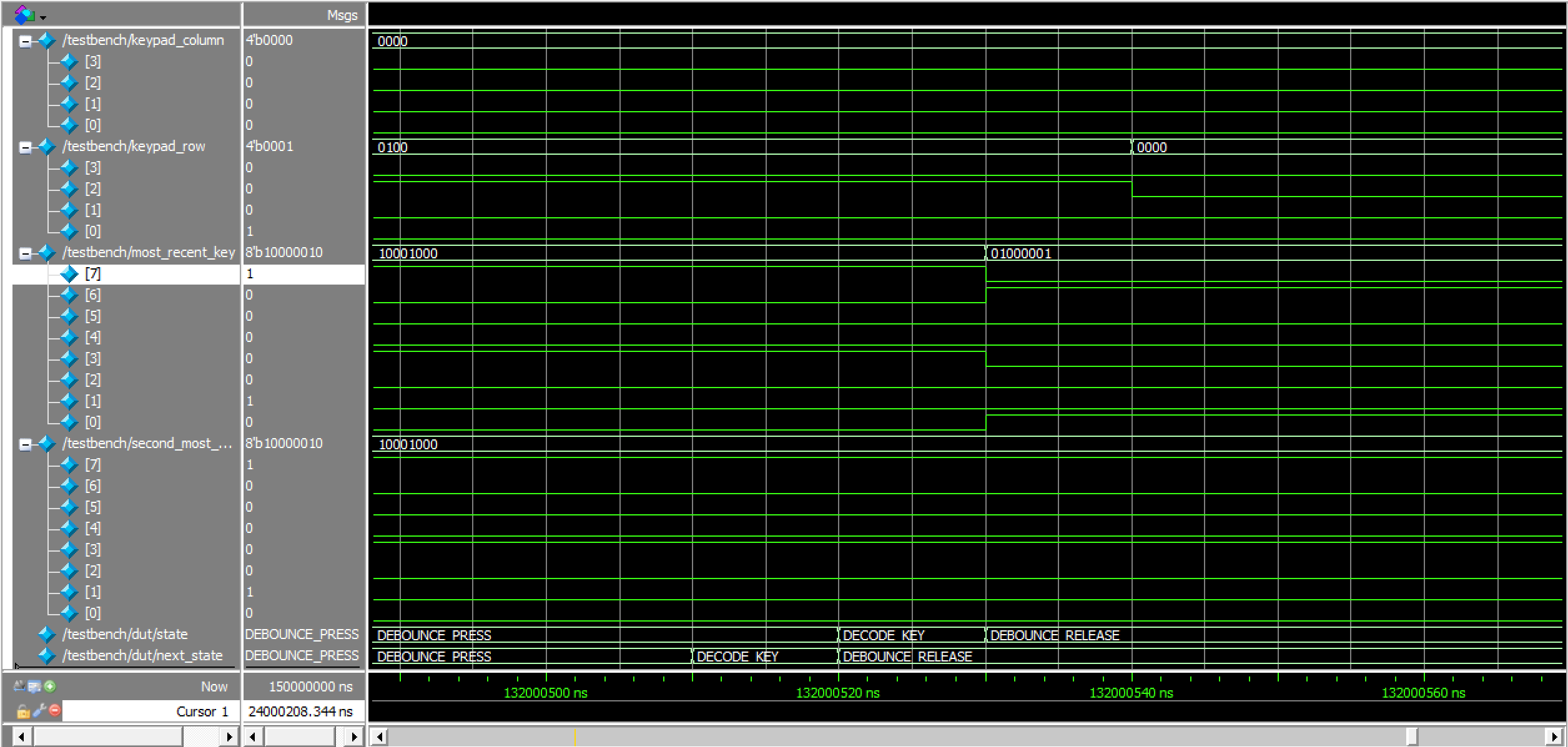
The keypad scanning and debouncing FSM waveforms can be viewed in Figures 8a, 8b, and 8c below. As expected, the FSM was in the correct state at any given point in time, and cycled through them appropriately in response to a variety of inputs, including a short, single key press, a prolonged key press, and key presses that occurred after an initial button was already pushed.
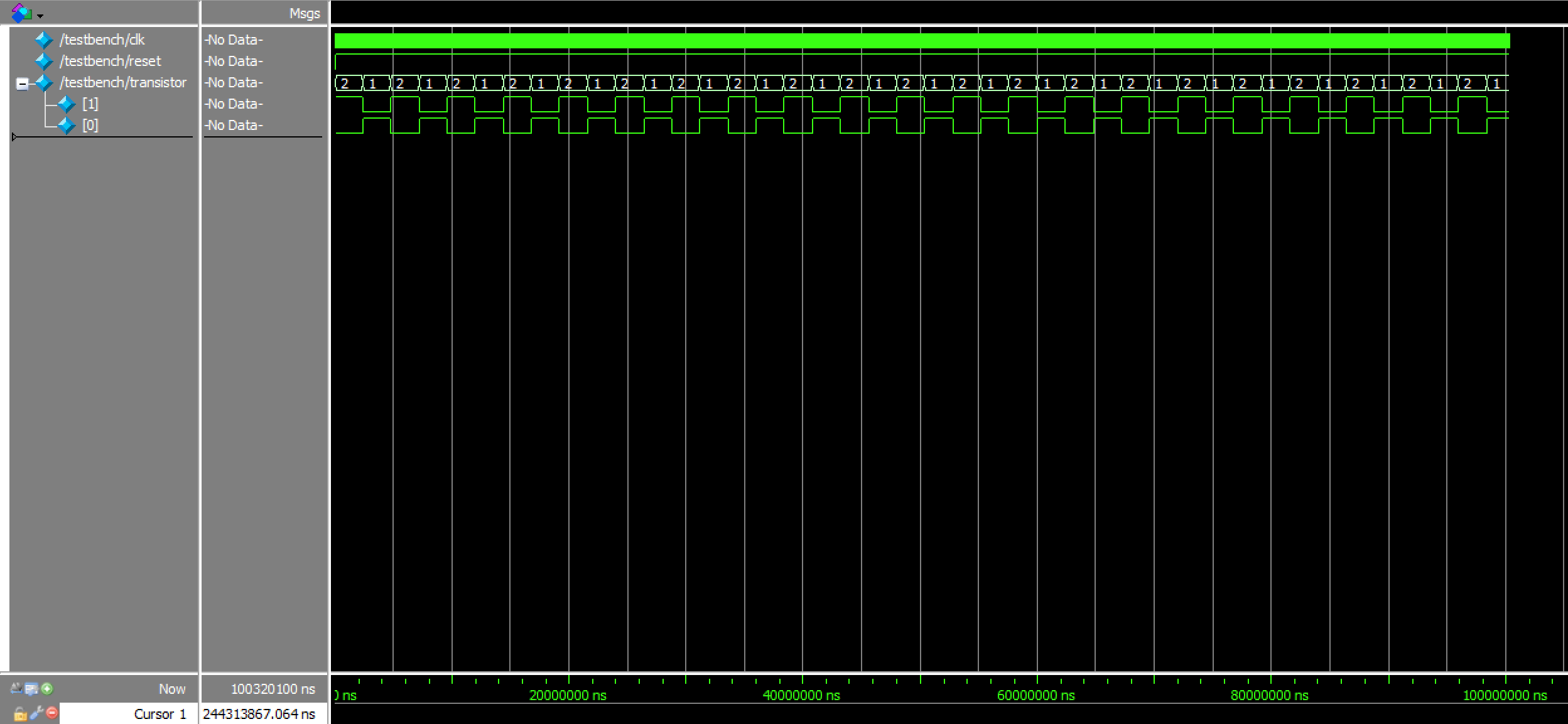
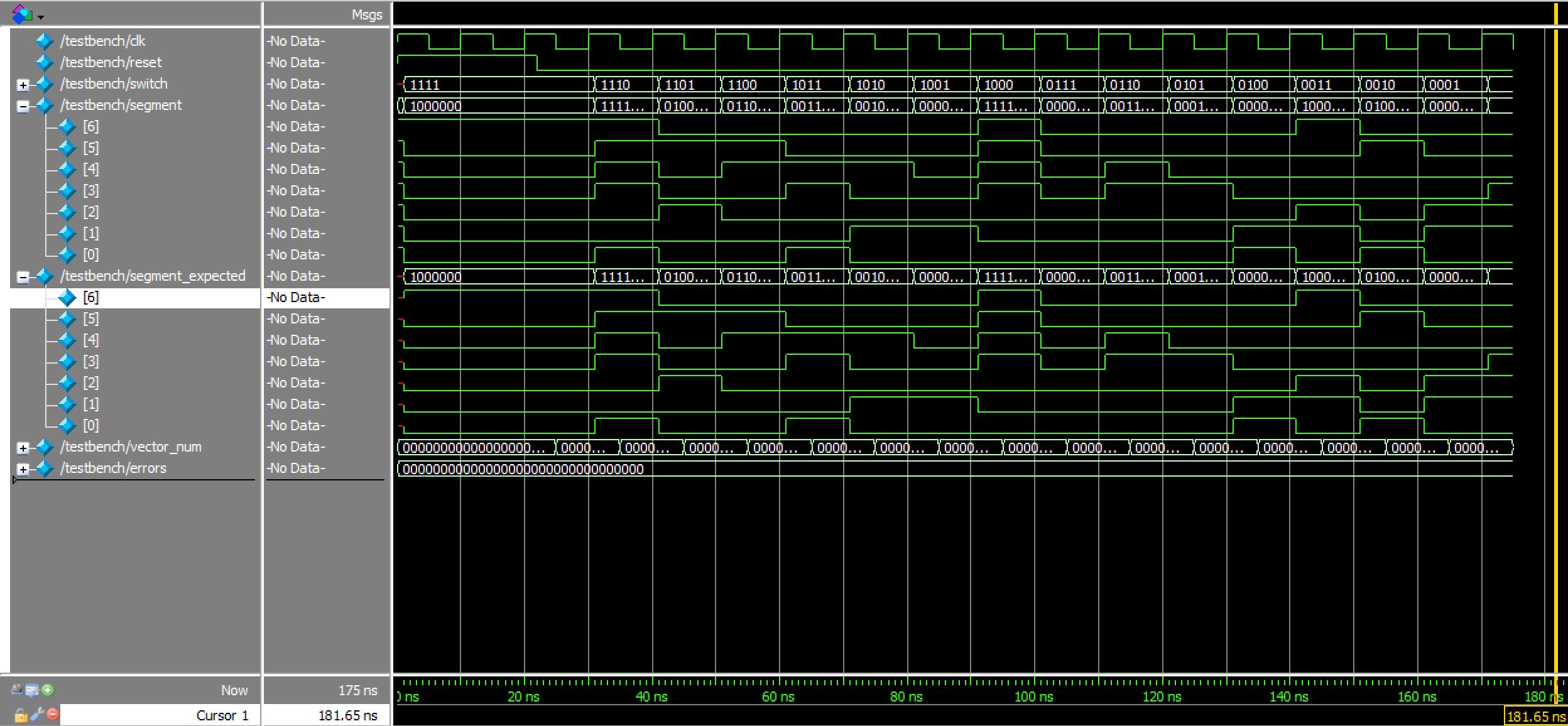
Moreover, the fact that all of these modules were tied together correctly can be verified more explicitly in Figures 9a and 9b, which depict the results of the top module testbench:
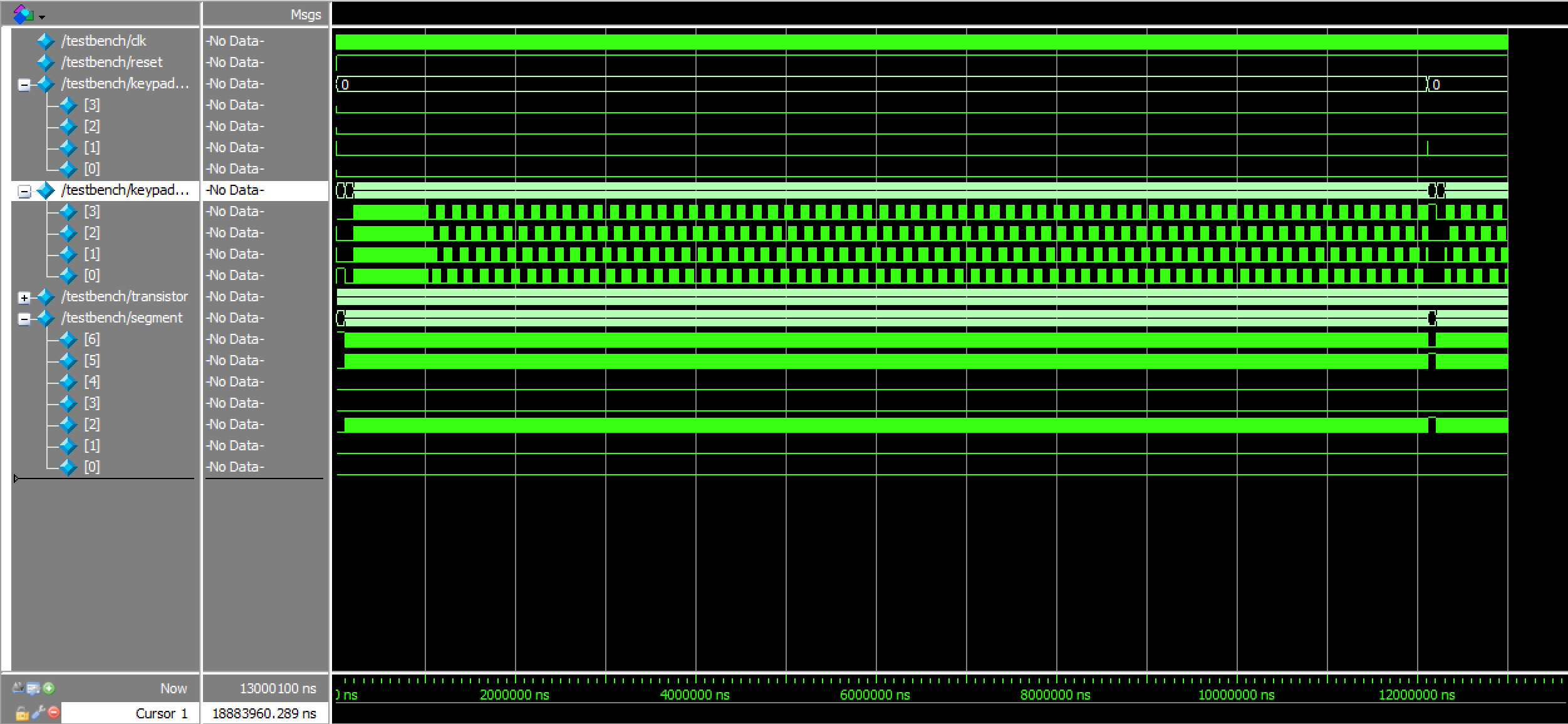
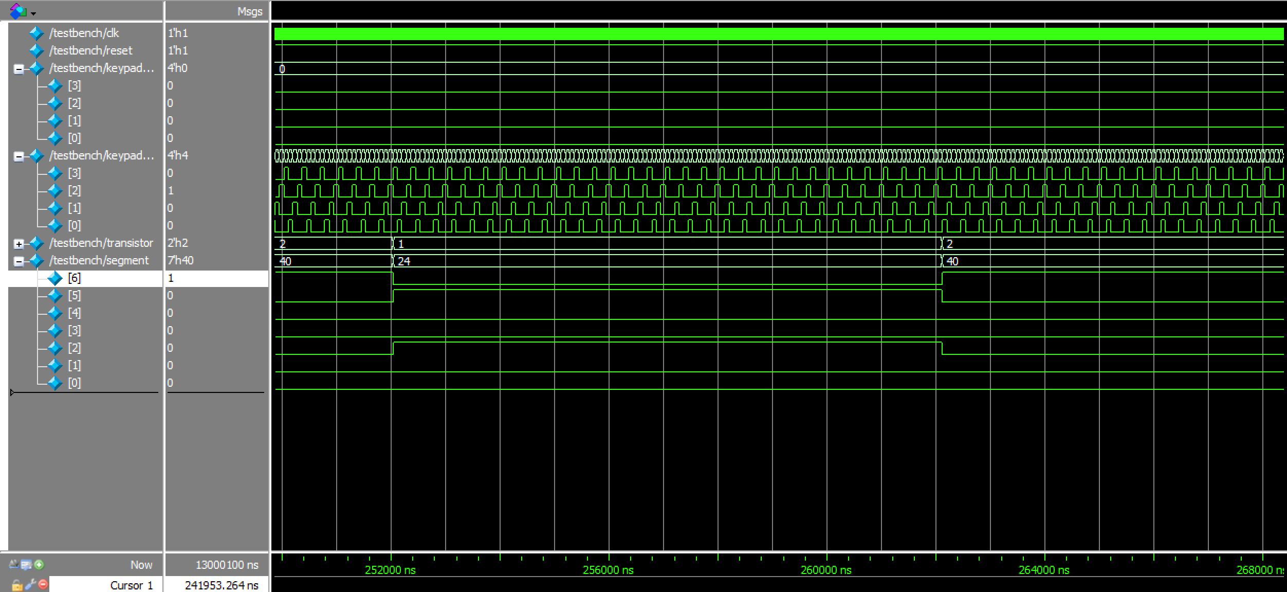
Because the top module took such an excessively long period of time to run — which was as intended with the integration of two 0.1 s (i.e. 10 Hz) long debouncing states, just unfortunate — only two key presses were actually simulated with it. However, due to the rigorous verification of all the submodules comprising it, this was deemed acceptable, as it still showed that everything was properly interfaced. Evidently, the cycling of which row is powered is shown, as well as the responses to such; when a column going high is detected, the waveforms also demonstrate that the correct toggling of the 7-segment display segments shortly follows (based on the value of output transistor).
Finally, as can be observed in the Figure 1 block diagram, there were also two 7-segment display-related modules used that — by proper verification standards — should have been simulated. These can be seen in Figures 10a and 10b below. Note that it is the exact same as the ones used in Lab 2.
All testbenches and simulations passed without the presence of any error messages.
Conclusion
In summary, the design dealt with all user inputs as appropriate, only registering each button press exactly once and only registering the first button press when multiple were active at the same time (until the initial one was released). Furthermore, the 7-segment displays never failed to accurately depict the two most recently pressed keys in the proper order, as outlined above, with no bleeding between digits; its time-multiplexed, 100 Hz toggling was also extremely consistent, with the display-switching going at a rate imperceptible to the naked human eye. A total of approximately 40 hours was spent working on this lab.
AI Prototype
Using ChatGPT to generate some code in response to the monolithic prompt “Target device: Lattice iCE40 UP5K FPGA with internal high-speed oscillator (~20 MHz). Write synthesizable SystemVerilog to scan a 4x4 matrix keypad and display the last two hex keys pressed on a dual 7‑segment display. Implement: A clock divider that derives a scan clock on the order of 100–200 Hz from the internal oscillator. A keypad scanning controller that iterates one active‑low column at a time and samples active‑low rows, registering at most one key per press (debounce‑by‑design), ignoring additional presses while any key is held, and allowing a new registration only after release. A top level that updates two hex digits (older and most recent) when a new key is registered and drives a time‑multiplexed two‑digit 7‑segment display without visible flicker and with balanced brightness. Use idiomatic SystemVerilog (e.g., logic, always_ff, enumerated states for FSMs). Provide clean module boundaries and keep all state synchronous. Include brief comments explaining the design choices,” the LLM produced results that surprisingly synthesized. These results can be viewed in the associated GitHub repository folder. Additionally, the full response can be seen in the public chat transcript.
While there were no actual errors in the AI code’s synthesis process, the corresponding warning messages can be viewed in Figure 11.

Additionally, ChatGPT was asked to respond to the second series of modular prompts, which can be viewed as follows:
“Target device: Lattice iCE40 UP5K FPGA. Overall Goal: Write SystemVerilog to scan a 4x4 matrix keypad and display the last two hex keys pressed on a dual 7 segment display. Current Goal: Write a synthesizable SystemVerilog module that produces a one‑shot registration signal for the keypad system. Behavior: When a key press is first detected, capture the current key code and assert a single‑cycle “new key” pulse. While any key remains pressed, do not accept additional keys. Only after keys are released should a subsequent press be recognized. This should handle debouncing of the keys. Implement as a small synchronous FSM with enumerated states and glitch‑free outputs. Keep names and interfaces reasonable; do not assume any hidden modules beyond what you define here.”
“Target device: Lattice iCE40 UP5K FPGA. Write a synthesizable SystemVerilog module that cycles through keypad columns (active‑low, one at a time) and samples rows (active‑low) to detect a single key at a time. Behavior: Iterate columns at a suitable scan rate derived from the divided clock and sample rows. When a key is detected, report a stable key code consistent with a standard 4x4 keypad layout and maintain it while the key remains pressed. Provide a boolean signal indicating whether any key is currently pressed. Use clean state encoding and synchronous logic; avoid combinational feedback and latches.”
“Target device: Lattice iCE40 UP5K FPGA with internal oscillator as the root clock source. Write a top‑level SystemVerilog module that instantiates the scanner and one‑shot modules, shifts the last two keys (older ← most recent; most recent ← new), and drives a multiplexed two‑digit seven‑segment display. Requirements: Update the displayed digits only when a new key is registered. Ensure equal apparent brightness and no visible flicker. Keep all logic synthesizable and synchronous; use idiomatic SystemVerilog constructs. Provide any small clock‑enable or divider logic you need. You can also assume that a sevenSegment module exists that takes a 4 bit input and outputs the 7 segments.”
The full response to these modular prompts can be seen in a second, entirely separate chat transcript.
Again, the AI’s design synthesized without error, and though the accompanying warnings can be viewed in Figure 12 below, nothing was visibly wrong with its end product upon first glance.

Overall, it can be concluded from this little experiment that providing an LLM with both monolithic and modular prompts results in generally similar behavior in the end — or, at the very least, for rather simplistic tasks.